May 31, 2026
May 31, 2026
THIS PROJECT HAS RISK OF SHOCK AND FIRE!
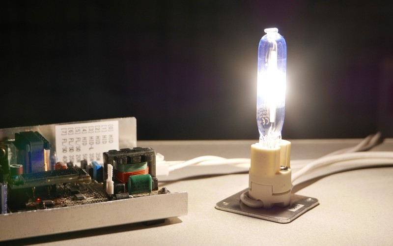
Low wattage CDM (ceramic discharge tube metal-halide) lamps in 70 watts and lower are designed to be driven in electronic ballast in order to drive the lamps at optimal condition. However the electronic ballast units for tiny CDM lamp, 15 and 20 watts, are quite rare in the market because they are mostly embedded in the luminaire. To obtain the low wattage ballast for the tiny CDM lamps, you will need to modify a 35 watts electronic ballast or build it yourself.
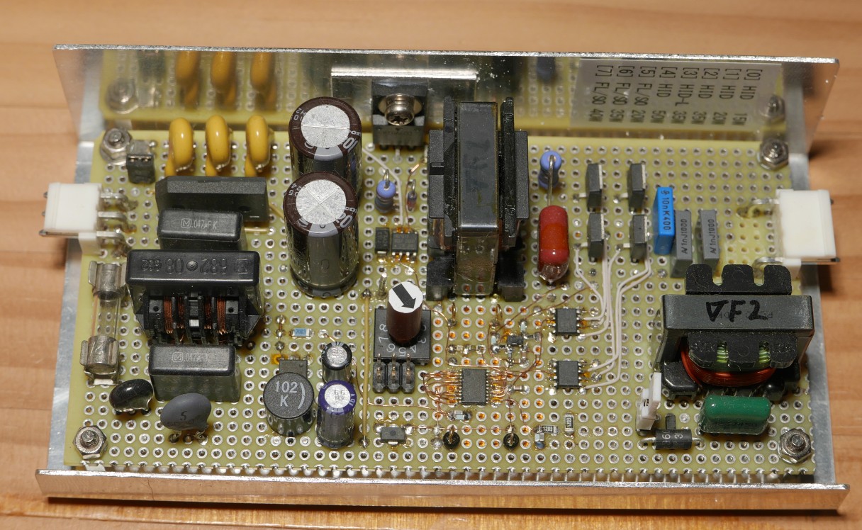
This project is a succession of the previous project to build yet another one. In this project, I have redesigned it based on the previous one to make it support the low wattage HID lamps in 50 watts and down to 15 watts. In addition, the circuit design is simplified so that every light bulb freak can build it if they have some experience in electronics.
This project is secondary to the previous HID Lamp Ballast project. Please refer to it for the fundamentals and basics on the discharge lamps and the lamp ballast.
The basic features in this project are based on the previous design. The supported lamp wattage is 15 watts to 50 watts, mainly small CDM lamps in G8.5, GU6.5 and PGJ5 base.Table 1 shows the specifications of built HID lamp ballast.
| Lamp Type | High-pressure mercury-vapor lamp, Metal halide lamp, High-pressure sodium-vapor lamp, (Low-pressure sodium-vapor lamp and Fluorescent lamp) |
| Lamp Wattage (PO) | 15-50 W in 8 presets. |
| Lamp Current (IO) | 0.8 A max. |
| Open-circuit Voltage (VO) | 280-320 V |
| Ignition Pulse (VIGN) | ≧ 3 kVPK |
| Controller | STM32L010 |
| Input Voltage (VI) | 110~120/220~240 V (2-voltage select), 50-60 Hz |
| Efficiency (η) | ~91 % (VI=115 V, PO=50 W, measured) |
| Power Factor (PF) | ~58 % (VI=115 V, PO=50 W, measured) |
The significant change of design from previous project is that the PFC feature is omitted and a capacitor input filter is used instead in order to make the circuit be simple and compact. The two input voltage range, low voltage mains and high voltage mains, are selected by a switch. For this reason, input power factor is quite low as shown in this table. Actually, every luminaire for general lightings in wattage of 5 watts and higher is classified into class C equipment under IEC 61000-3-2. Especially, an active PFC is virtually mandatory for the luminaires over 25 watts. However, since this is a one-off project and the wattage is not that so high, so that I decided to omit the PFC feature in this design.
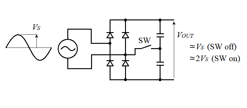
This project omits a PFC filter and employs a traditional capacitor input filter. In this type of filter circuit, the filtered output voltage varies directly depends on the input voltage, and the bus voltage will change drastically, between 120 and 370 volts, when it supports universal voltage. However, common drive circuit in HID lamp ballast requiers a bus voltage of 300 to 400 volts, so that the bus voltage is not sufficient at the low voltage mains. To solve this problem, I made the rectification circuit able to be changed in rectification mode, full-wave mode for high votage mains and voltage doubler mode for low voltage mains. This configuration was often used in dual voltage PC power supplies in old days and it can be achived by only a single contact switch as shown in Figure 1.
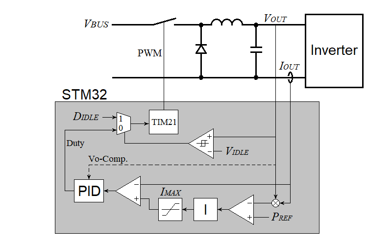
This block works as the lamp ballast. It steps-down the bus voltage and regulate the lamp current at the commanded level. Figure 2 shows the control diagram of the buck converter.
The buck converter works in constant power mode to regulate the output power at the rated lamp wattage, so that it feeds-back not only output current but also output voltage. The lamp current control, the minor feedback loop, need to be in fast respose and the PID gain can be tuned for each lamp configuration. The lamp power control, the major feedback loop, needs to be accurate, but it does not need to be in so fast response. Too fast response of major loop leads the minor loop unstable and causes flicker of light, so that it may be in only I control.
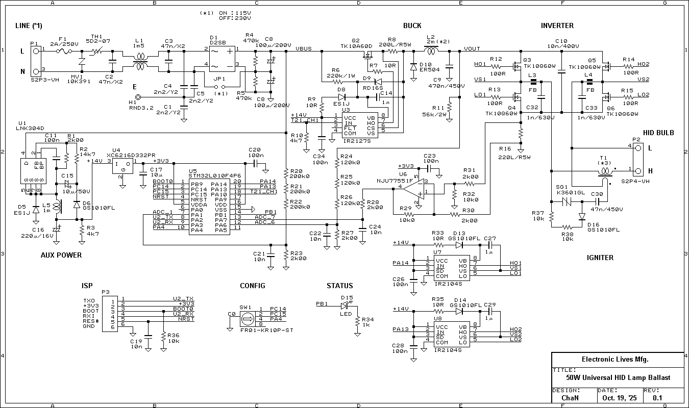
When the buck converter is in idle mode that the lamp is not in discharge and the output voltage sticks high, the feedback control is disabled and the transistor is driven at a fixed PWM waveform. This is to keep the inductor at freewheel operation (the voltage at switch node drops to zero every switching cycle) so that the bootstrap capacitor C14 of gate driver can retain the charge. The bleeder resistor R11 is to achieve this operation. When the buck converter is not in work, C14 is charged via a current path R6→C14→R11.
When the lamp breaks-down and begins discharge, the output voltage drops and the buck converter enters normal operation mode. On this mode transition (not illustrated in the diagram), an inrush current is output without control for certain time to make the arc stable. Even without contorl, the transistor will not fail because the excessive current is limited by a trip feature of the gate driver.
The lamp wattage and the control parameters can be preset for eight different lamp types. The lamp type can be selected with a rotaly switch SW1.
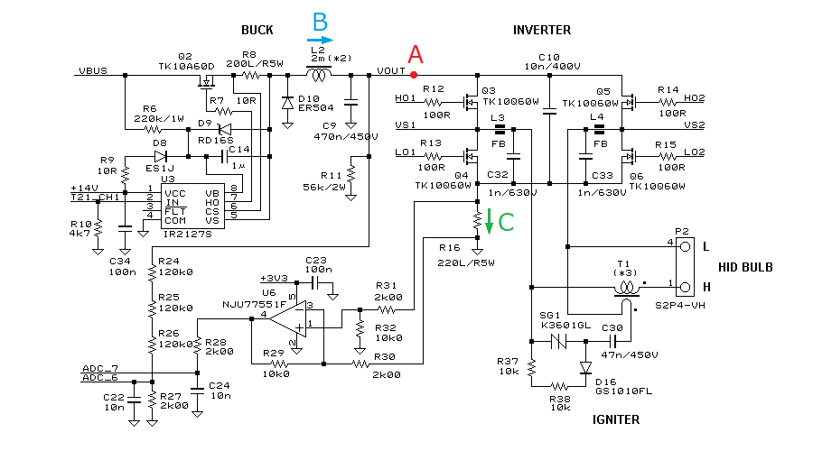
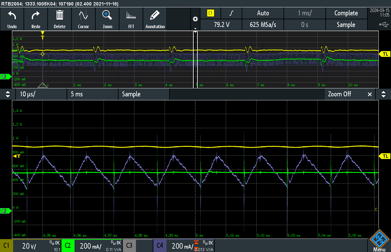
Figure 3 shows the schematic of lamp driver part and Figure 4 shows the working waveform of buck converter. L2 is an inductor in a pair of EE ferrite cores B66317GX187 (gap = 0.3 mm) and 120 turns of 0.5 mm UEW. It makes L = 2 mH and ISAT = 1.5 amperes. Any power choke inductor in equivalent specs will work well. The colored symbols in the schematic are the probing points of waveforms, A for output voltage (Ch1), B for inductor current (Ch4) and C for output current (Ch2). The ripples appear at the output in period of 2.5 ms are from the turbulence of current control due to switching operation of inverter and inductance of igniter. The waveform of inductance current looks noisy is due to a poor noise performence of current sensor used as a current probe.
Every HID lamp for generic lightings has symmetric electrodes to be driven in AC, so that the DC output of buck converter needs to be converted into AC with an H-bridge inverter and supplied to the lamp. The switching frequency of inverter is commonly set between 100 Hz and several hundreds Hz because the frequency cannot be over 1 kHz due to there is an igniter (an inductance) in series and to avoid acoustic resonance. This scheme is known as LFSW (Low Frequency Square Wave) drive and it has advantages that high lamp efficacy and no flicker as DC drive. In this project, the lamp is driven at typical switching frequency, 200 Hz.
The output voltage sticks the saturated level, 250 to 300 volts, while the lamp is not in discharge. The SIDAC SG1 (VB = 360 volts) triggers when the output voltage is 180 volts or higher and pulse current at every alternation of inverter output is flow through the primary winding of the ignition transformer T1. The secondary winding is in series of the lamp, so that the high voltage pulses added on the inverter output are applied to the lamp.
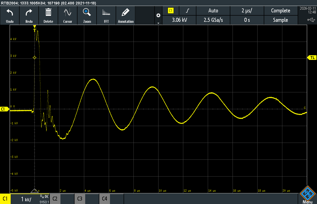
The JIS C 7629 standard lists the specifications of some typical HID lamps for the design of lamp ballasts, and also the peak value of ignition pulse and accumulated pulse width are presented in the specifications. From this standard, most pulse start type HID lamp requires higher than 3 kV of peak voltage but lower than 5 kV for a safety. The accumulated pulse width is the pulse density for steady start-up and the most lamp requires 100 μs/s at least. The breakdown between the electrodes occures on an ionization of gas atoms caused by cosmic ray while a high voltage is applied. For this reason, a certain pulse density is requierd for the steady start-up, especially small discharge tube in low wattage lamps.
T1 is the ignition transformer in an EI ferrite core PC40EI25-Z (gap = 0.2 mm), 8 turns of 0.4 mm wrapping wire (13 μH) and 70 turns of 0.5 mm wrapping wire (1 mH). Figure 5 shows the waveform of ignition pulse with output opened. The ignition pulse is attenuated by stray capacitance on the cable, so that every electronic ballast specifies the maximum cable length between ballast and lamp, commonly 1.5 to 2 m. In this circuit, the peak voltage is over 4 kV and the pulse density is 160 μs/s. There is not any control of igniter but the SIDAC stays off state and stops ignition pulse when the lamp begins discharge and the lamp voltage drops.
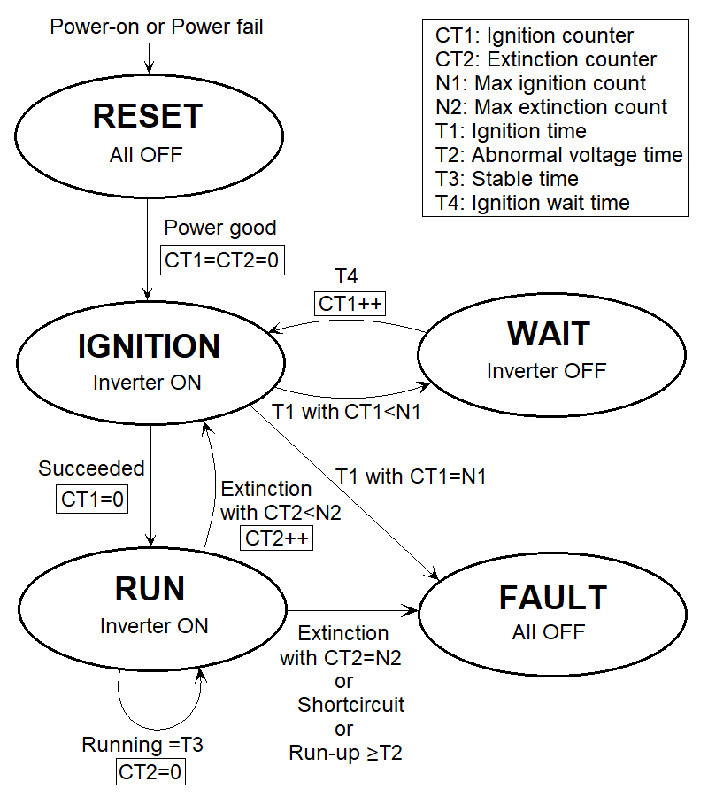
The HID lamps can get into an abnormal condition when it reaches end of life. The HID lamp ballast need to shut-down safely when such a condition is detected. For the steady start-up and operation of HID lamp, a control state diagram is defined as shown in Figure 6 to manage the system.
The control get into this state on power-on and BOD (low VBUS). After the VBUS reached a certain level, CT1 and CT2 are cleared and then the control state changes into IGNITION state.
Lamp ignition. To start the ignition, the buck converter and inverter are enabled. When a success of take-over is detected (output voltage lowers by stable arc discharge), CT1 is cleared and the control get into RUN state. If T1 time is elapsed while a stable discharge of lamp is not detected and CT1 < N1, CT1 is incremented and the control state changes into WAIT state. If CT1 = N1, the control get into FAULT state (lamp EOL or no lamp).
Lamp is discharging and the lamp voltage is monitored continuously. When the lamp warms-up and the discharge tube reaches thermal equibilium, the lamp voltage will get into the regular range. If it is not in normal voltage range for T2 time, it is judged an abnormal lamp voltage and the control state changes into FAULT state. This is caused by incomplete warm-up due to leakage of outer tube, insufficient pressure of discharge tube due to leakage of discharge tube, voltage rise on EOL or wrong lamp wattage. If a short-circuit is detected, it also changes into FAULT state. If an extinction is detected, the control state changes into IGNITION state if CT2 < N2. If it is too many restart (CT2 = N2), it is judged the lamp is unable to run stably and the control changes into FAULT state. When T3 time elapsed in this state, it can be considerted steady operation and CT2 is cleared.
To limit the continuous output of ignition pulse, the inverter is disabled for T4 time and then the control changes into IGNITION state.
An abnormal condition of lamp or a failure of wiring has been detected. All function is shutdown.
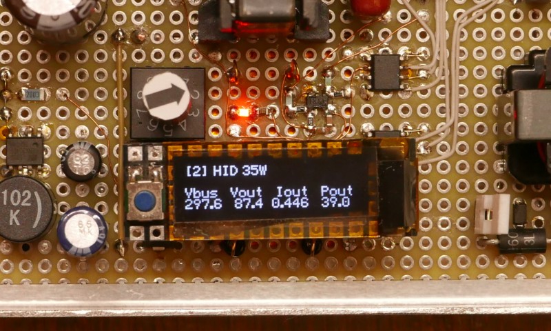
The circuit board has a programming connector which includes a UART interface and some control lines. It can be used for not only memory programming but also monitoring the working status under normal operation. In addition, the working parameters can be dynamically changed by command inputs. Of course an isolation transformer or an isolated UART adapter is needed to attach the PC to a non-isolated circuit safely.
I had thought that it is tiresome to bring a PC to monitor the UART output and built a tiny display module shown in Figure 7. It is a simple serial display that is pulged on the programming connector and can display received data from TXD pin into OLED in 20 columns by 4 lines. The push switch pulls down the RXD pin, also read as GPIO, to send simple commands to the controller. In this project, the lamp wattage can be adjusted in ±1 watt step by button hold time, 100 to 400 ms to decrease and 400 to 800 ms to increase.
The display module pulls 20 mA from the target board and does not need an extra power supply for the module. If the programming interface is unified in your projects, a same module design will able to be used for every target borad. I noticed that it is useful and worte an article about the tiny display module as an separated article here.